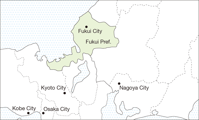
Today, smartphones and other electronic devices have become ubiquitous, but this would never have been possible without incredible advancements in plating technology. Plating processes, which apply a metal coating to the surfaces of other materials, not only improve the appearance of everyday manufactured products and enhance their durability, but are also essential in producing the circuits in all sorts of electronic devices. When Kiyokawa Plating Industry Co., Ltd. was founded in Fukui City, Fukui Prefecture in 1963, its primary business was the coating of wheel parts for automobiles and motorcycles, but in the 1970s the company began to focus on plating for electronics and has since grown significantly due to its highly specialized technology and expertise in the field. Although Kiyokawa Plating Industry remains a small-tomedium enterprise with 270 employees at present, its unique nano-plating technology is a pillar of Japan’s electronics and semiconductor industries and many consumer products exported to the rest of the world feature plating by the company.
Main advantages of metal plating
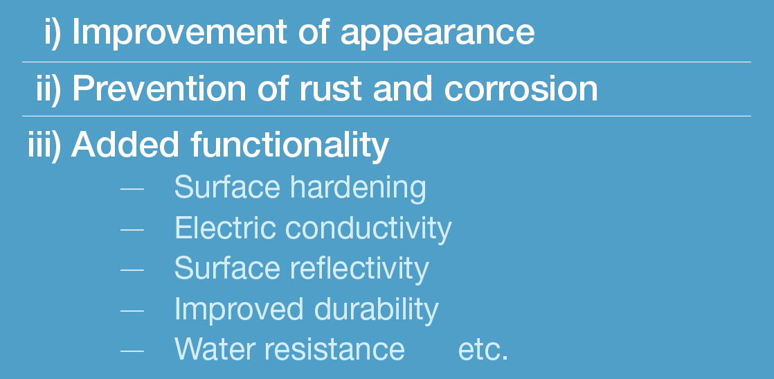
Metal plating is used for various purposes. One of these is the preservation of material properties during the production of parts via a special plating that dissolves completely once a finished part has been assembled.
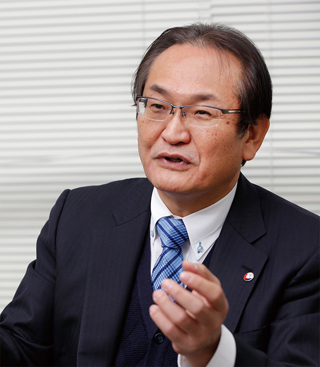
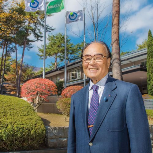
Dr. Hajime Kiyokawa
President and CEO of Kiyokawa Plating Industry Co., Ltd. Born in 1964 in Fukui Pr e f ectur e. Graduated from University of Fukui Graduate School in 1989, and joined Fujitsu Limited the same year as a semiconductor engineer. Joined Kiyokawa Plating Industry in 1991 and has been serving in his present position since 2010.
What makes nano-plating technology special is that it makes it possible for factors like coating thickness and structure to be controlled in nanometer units. Another advantage over other companies’ approaches is the ability of this technology to make use of the unique characteristics of both the base material and the coating material. President and CEO Hajime Kiyokawa explains that “nano-plating technology has enabled the plating of extremely delicate electronic parts and semiconductor chips. Our technology thus contributes to the miniaturization and weight reduction of electronic devices such as cell phones, and has made it possible to manufacture ever-thinner batteries even as their capacities increase.”
Since Kiyokawa Plating Industry’s founding, its DNA has expressed itself in the free-thinking development of new technology and the willingness to make the investments necessary for such advances. The company entered the electronic parts sector after its founder and Executive Chairman Tadashi Kiyokawa read about semiconductors in an economics journal and recognized the immense potential for growth in this worldchanging industry. He then took it upon himself to study the equipment that was being used in the electroplating of miniature parts at that time and was able to find ways to improve the designs. Optimizing plating conditions through the use of self-produced materials of uniformly high standard, the company achieved inexpensive mass production with consistent quality. In 1982 it also established an internal Science and Technology Institute. Along with the use of various devices to measure and analyze the plating process, this has led to a near-zero fault rate.

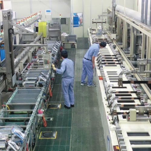
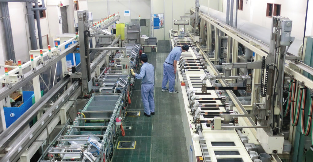
Roughly 30 of Kiyokawa Plating Industry’s approximately 270 employees work in research and development. About 70% are nationally certified as plating technicians, pollution control managers, or handlers of poisonous and deleterious substances.
According to the CEO, Kiyokawa Plating Industry’s track record of having developed numerous proprietary technologies has led its clients to sometimes submit development requests so difficult that they appear impossible. The company rarely turns down requests, however, and often takes on a project even if it requires several years of development. CEO Kiyokawa explains, “Our pride and curiosity as engineers drives us to accept the challenge of difficult requests. Considering that seemingly wasteful processes of trial and error can eventually lead to marketable technologies and expertise, we don’t let short-term profitability guide our decision-making. We once tasked a new hire with a certain development request. He tried out methods that more experienced engineers had rejected as being too improbable to succeed, and he managed to find a clue for solving the problem that way. In order to accomplish something that has never been done before it’s important to be open to things that may seem like a waste of time at first.”
Kiyokawa adds that “plating technology is a fascinating subject, as there are still aspects of it that are difficult to explain theoretically and many new discoveries to be made. Cutting-edge advancements in plating can contribute to biotechnology, medical treatment, and countless other fields. I hope that we’ll never lose touch with our spirit of exploration, so that we can continue to develop creative new technologies.”